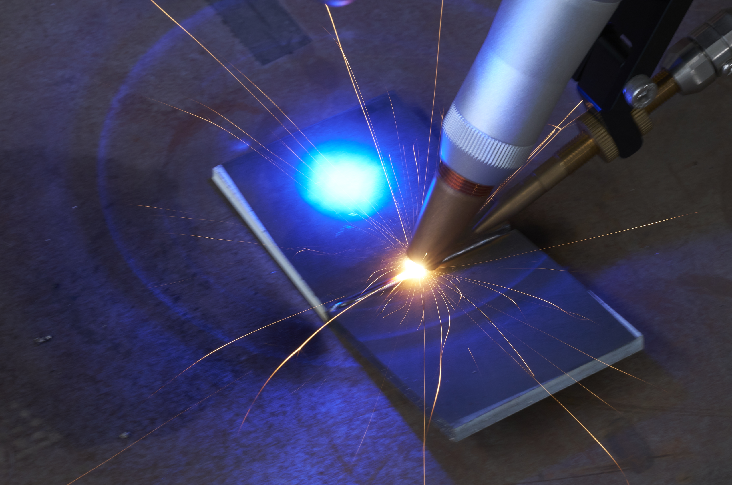
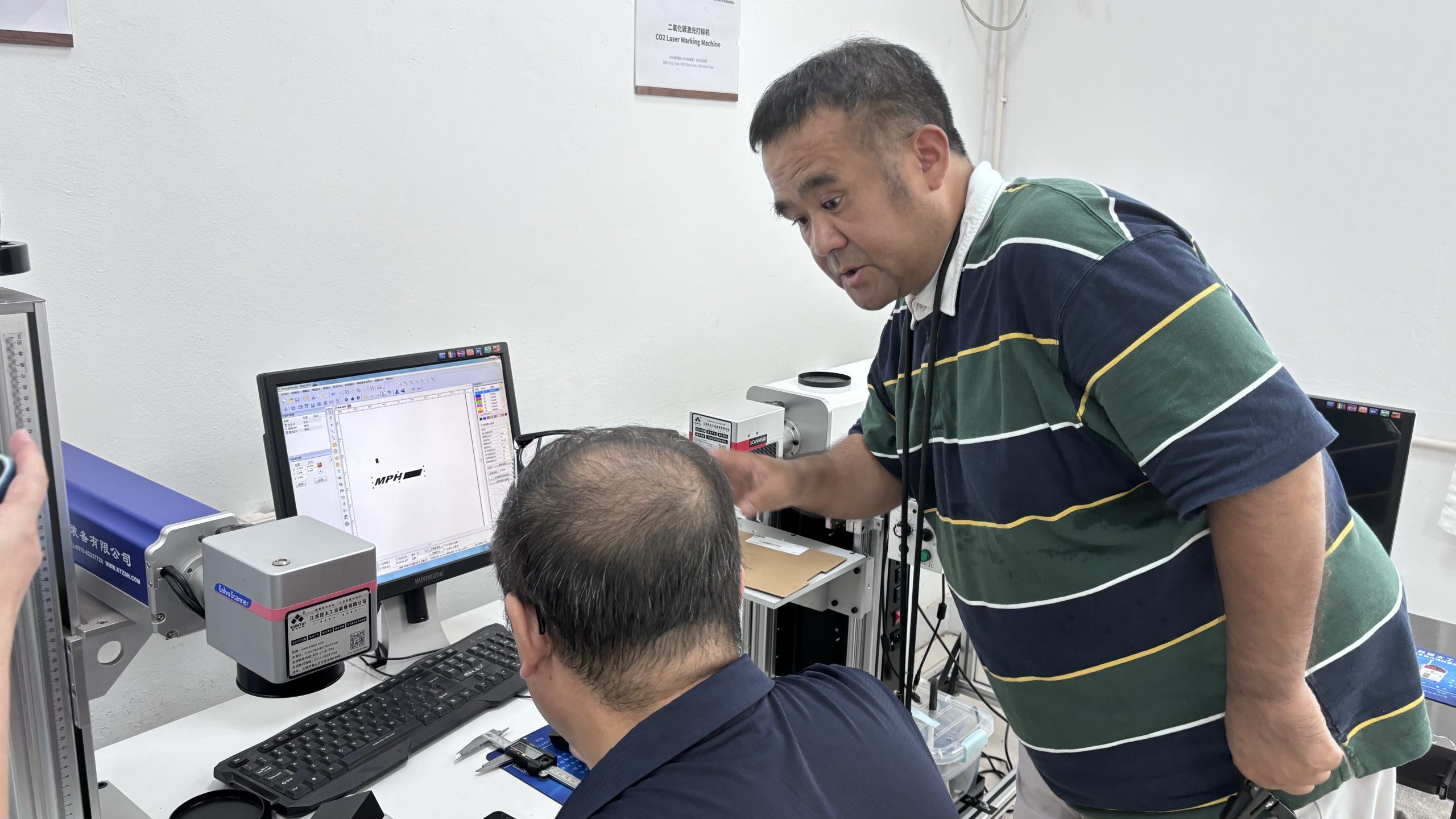
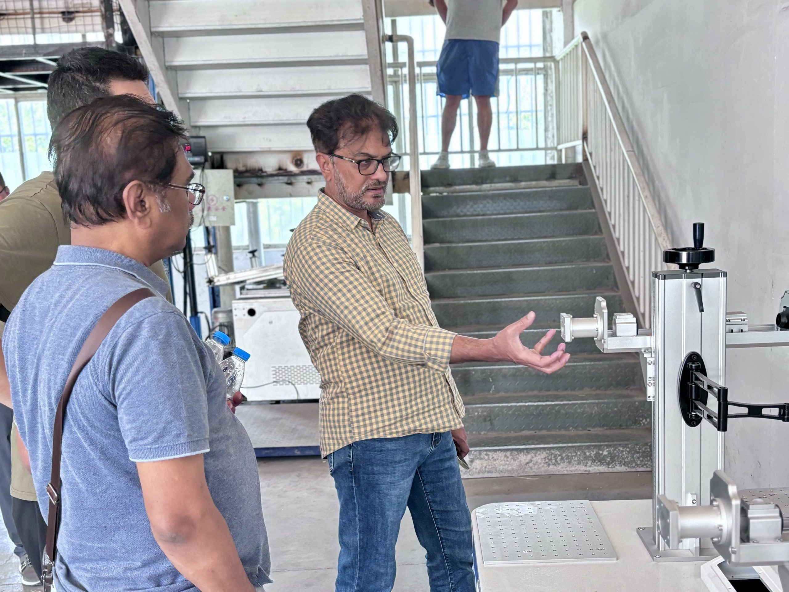
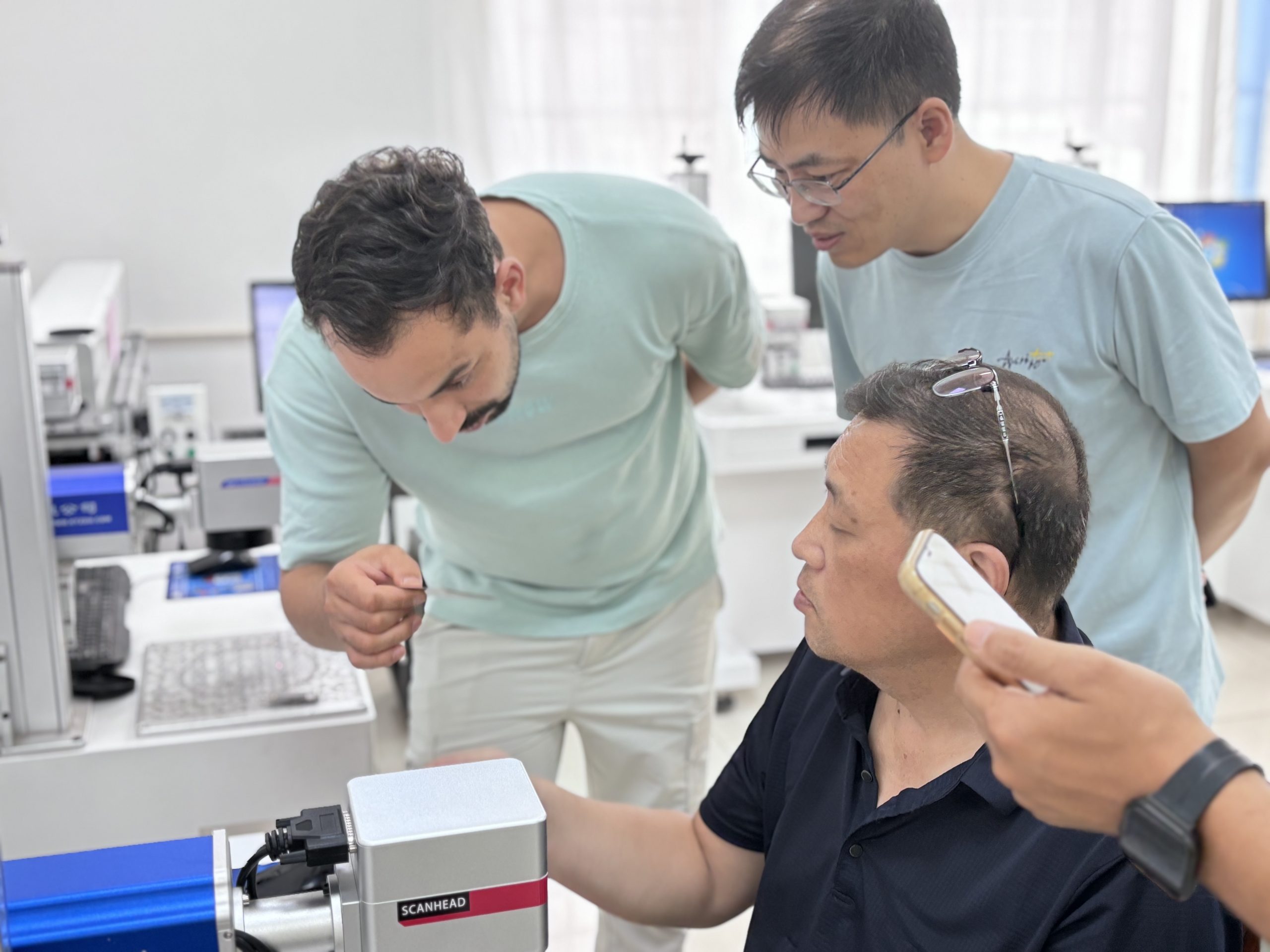
As demands for precision and traceability grow in PCB production, traditional marking methods can no longer meet the requirements for accuracy, durability, and environmental safety.Laser marking, with its non-contact process and high precision, enables micron-level engraving of codes and patterns on PCB surfaces—efficiently, permanently, and without pollution.
This article outlines the core principles, advantages, and prospects of laser marking as a key technology in modern electronics manufacturing.
· PCB’s “Smart ID Card” Generator
1. Permanent marking of proprietary information
Each PCB has its own “ID card” – QR code, serial number, LOGO. Traditional ink printing is easy to wear, while laser marking directly “burns” permanent marks, which cannot be wiped off even at high temperatures and corrosion! Industry pain points solved in seconds: Scan the code to trace the faulty batch when repairing a mobile phone? Track the life of automotive electronic components? It all depends on it!
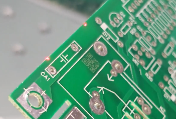
2. Accurate to microns
Modern PCB components are often too small to be distinguished by the naked eye. Traditional mechanical engraving methods pose a high risk of damaging delicate structures. In contrast, laser technology enables highly precise, non-contact marking—capable of engraving over 100 characters within an area no larger than a fingernail, without affecting surrounding circuits.
A game-changer for flexible printed circuits (FPCs): Found in foldable smartphones, FPCs are as fragile as insect wings. Laser processing, with its non-invasive nature, eliminates mechanical stress, making it the ideal solution for such ultra-thin and sensitive substrates.
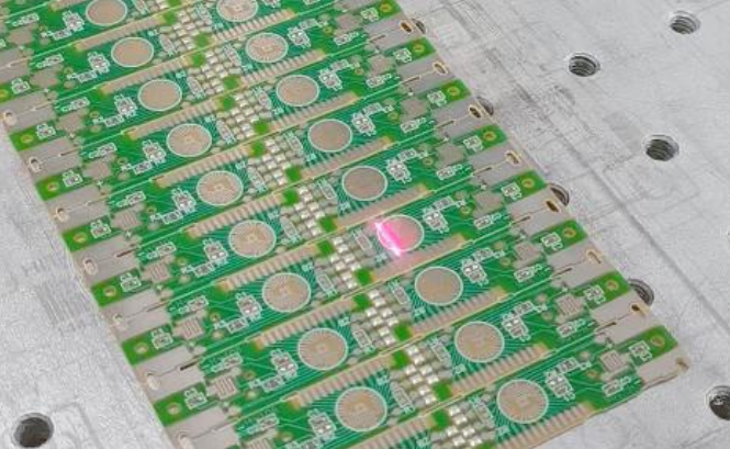
· Three core advantage
1. Traditional mechanical tools often deform thin sheets during processing. In contrast, laser technology operates without physical contact, allowing for precise and reliable marking even on ultra-thin PCBs as slim as 0.2 mm.
2. Traditional mechanical tools often deform thin sheets during processing. In contrast, laser technology operates without physical contact, allowing for precise and reliable marking even on ultra-thin PCBs as slim as 0.2 mm
3. Laser marking requires no ink or chemical agents, significantly reducing the use of consumables. It fully complies with environmental protection standards, eliminating concerns over wastewater and harmful emissions.
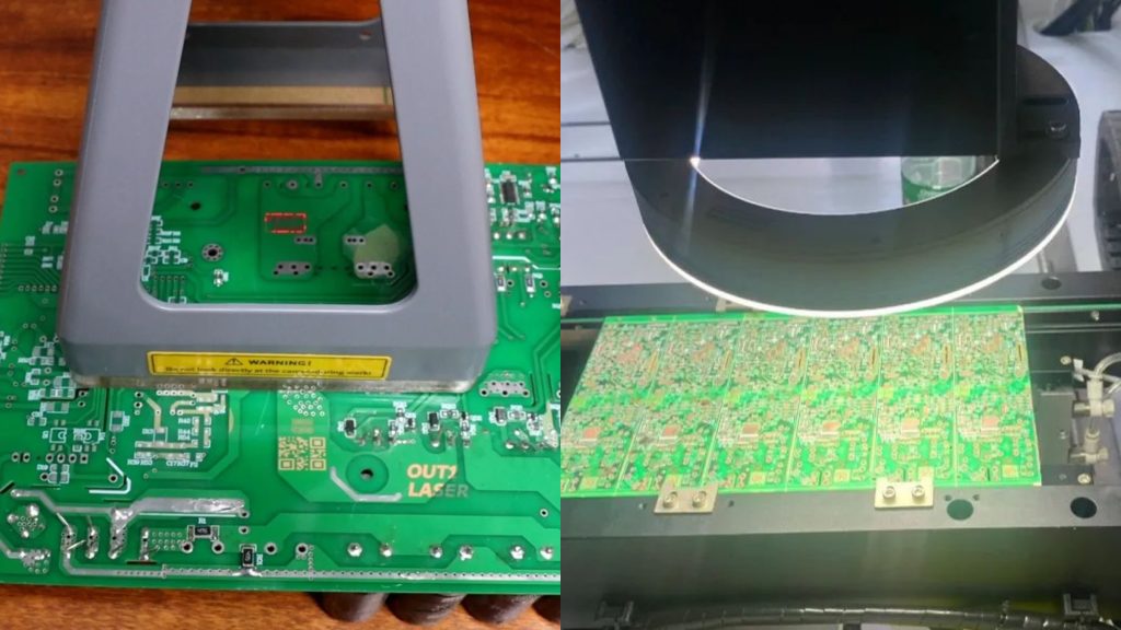
· Black technology
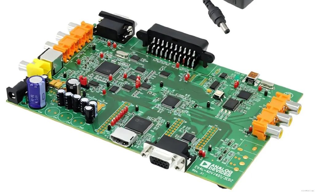
Cold Processing: Ultraviolet (UV) laser marking utilizes a “cold processing” mechanism, where the material is vaporized instantly with minimal heat generation. This effectively prevents thermal damage to sensitive electronic components.
Micron-Level Depth Control: Marking depth can be precisely controlled at the micron scale—deep enough to penetrate the solder mask and reveal the copper layer, yet without damaging the underlying circuitry. (Illustration: Examples of different marking depths)
Invisible Anti-Counterfeiting: By using specific laser wavelengths, markings can be rendered invisible under normal conditions but become instantly visible under designated light sources—providing a powerful anti-counterfeiting solution that is nearly impossible to replicate.
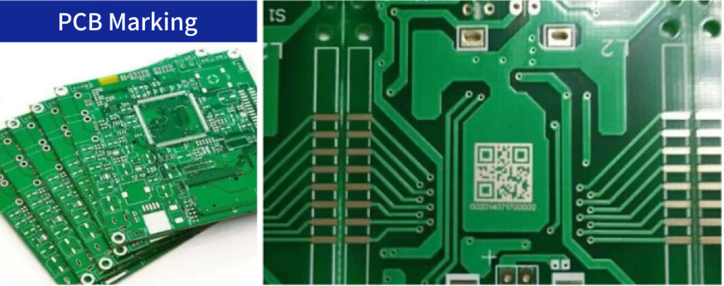
The adoption of laser-marked QR code technology in the PCB industry enables full traceability of production, process, and quality data, while supporting automation and intelligent management. This meets the demands of lean manufacturing, quality control, and process optimization.
Marking QR codes on PCB surfaces has become a common requirement among mid-to-high-end customers and is now widely implemented across the industry.
Kuntai Laser’s solutions empower PCB manufacturers to achieve comprehensive traceability and intelligent management throughout the production lifecycle, fully aligning with modern manufacturing standards and quality assurance needs.
